A Harvard architecture CPU uses separate paths for instructions and data. In a classic implementation, program instructions and working data also live in separate address spaces. That organization can let the processor fetch its next instruction while it reads or writes data, reducing one source of memory contention.
The word can matters. Separate paths create an opportunity for concurrent access; they do not guarantee twice the speed, fixed timing, or lower power. Caches, shared interconnects, external memory, pipeline stalls, and the program itself still determine the result. This guide explains the useful model, the common modified version, and the checks an engineer should make in a real data sheet.
Harvard architecture CPU: key takeaways
- Separate access paths are the core idea: the processor can have one interface for instruction fetches and another for data reads and writes.
- Pure and modified Harvard designs are different: a modified design often has split instruction and data caches above unified main memory.
- Performance depends on implementation: separate paths remove one conflict, but they do not remove every bottleneck.
- The data sheet is decisive: look for address maps, bus interfaces, cache rules, tightly coupled memory, and program-space access instructions.
What is Harvard architecture?
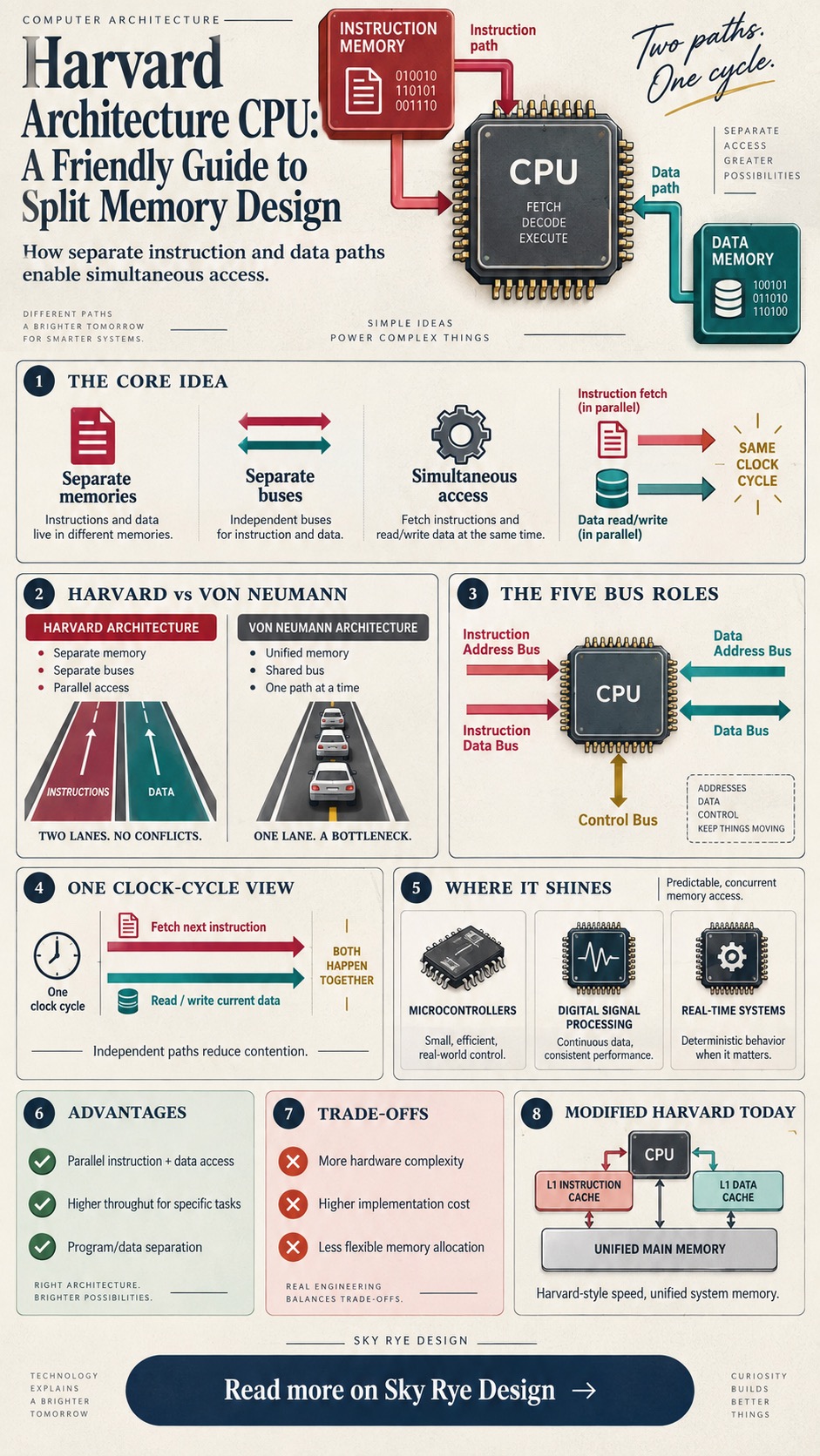
Harvard architecture is a processor and memory organization in which instructions and data use separate storage domains and access paths. The program counter selects an instruction from program memory while load and store operations address data memory. Because those transactions do not have to use one shared interface, they may proceed in the same processor cycle.
The name comes from the Harvard Mark I tradition. The Computer History Museum identifies the IBM Automatic Sequence Controlled Calculator, also known as the Harvard Mark I, as a 1944 electromechanical machine. That historical machine is not a blueprint for every modern microcontroller, but it explains the terminology. See the museum’s Harvard Mark I artifact record.
How the instruction and data paths work
A simple example helps. Suppose an instruction adds a value from memory to a register. The instruction side fetches and decodes the add operation. At the same time, the data side can read the operand from data memory. In a design with one shared path, those requests may need to take turns. In a Harvard-style design, independent interfaces can serve them concurrently.
| Part | Role | What to verify |
|---|---|---|
| Instruction memory or cache | Stores or supplies executable instructions | Address range, width, cache line size, wait states |
| Data memory or cache | Holds variables, stack data, and buffers | Read/write width, alignment, latency, coherency rules |
| Instruction interface | Carries fetch addresses and returned instruction bytes | Whether it reaches flash, cache, TCM, or a shared bus |
| Data interface | Carries load and store transactions | Which memories and peripherals it can reach |
| Control and execution logic | Decodes instructions and schedules operations | Pipeline behavior, stalls, hazards, and memory ordering |
Arm’s description of the Cortex-M3 is a concrete example: the core uses a Harvard architecture with separate instruction and data buses, so instruction fetches and data accesses can occur in parallel. The same official overview also shows why one label is not enough; the core connects those interfaces to a wider bus system. Read Arm’s Cortex-M3 core tour.
Harvard vs Von Neumann architecture
The textbook distinction is about how instructions and data share memory resources. It is not a ranking in which one architecture always wins. A unified Von Neumann address space can simplify memory allocation and program loading. Separate Harvard paths can increase available bandwidth for workloads that fetch instructions and move data at the same time.
| Question | Classic Harvard | Classic Von Neumann | Modified Harvard |
|---|---|---|---|
| Instruction and data address spaces | Separate | Unified | Often unified for software, split near the core |
| Access paths | Separate instruction and data paths | One shared path in the simple model | Separate L1 instruction/data paths, shared lower levels |
| Concurrent access potential | Yes | Limited by the shared interface | Yes when accesses hit separate local resources |
| Memory flexibility | Program and data capacity are less interchangeable | One pool can hold code or data | Depends on cache and memory-map design |
| Common concern | Program-space access and hardware complexity | Instruction/data contention | Cache coherency and maintenance |
This comparison is architectural, not a promise about a product. An advanced Von Neumann processor can use caches, prefetching, wide buses, and out-of-order execution to sustain high throughput. A small Harvard microcontroller can still wait on slow flash. Compare the whole memory hierarchy rather than treating the label as a benchmark result.
Why separate paths can improve performance
Instruction fetch and data access can overlap
The most direct benefit is removing a structural conflict: the fetch unit does not necessarily have to wait for a load or store to release the same path. That helps pipelines keep their next instruction ready, especially in loops that repeatedly read samples, coefficients, pixels, or control data.
Each side can be tuned for a different job
Instruction storage may favor sequential reads and a width that matches encoded instructions. Data memory needs reads and writes, byte handling, and access to peripherals. Separate interfaces let a designer choose widths, protection rules, cache policies, and local memories that suit each traffic type.
Local memories can make timing easier to analyze
Some embedded processors include instruction and data tightly coupled memories, often called ITCM and DTCM. Arm’s Cortex-M7 data sheet lists configurable instruction and data TCM as well as separate instruction and data caches. Those local memories can avoid some cache uncertainty, but deterministic timing still depends on placement, bus traffic, interrupts, and the platform integration. See the official Arm Cortex-M7 processor data sheet.
Trade-offs engineers need to manage
- More interfaces and control logic: separate paths require arbitration and integration with caches, flash, SRAM, DMA, and peripheral buses.
- Split capacity: unused program memory cannot automatically become data memory in a pure design, or vice versa.
- Special program-space access: constants stored with code may need special instructions, mapping windows, or library support.
- Toolchain awareness: linker scripts must place code, constants, stacks, and buffers in regions the relevant interfaces can reach.
- Coherency work: a modified Harvard core may need explicit cache maintenance after code is generated or modified.
These trade-offs are why it is inaccurate to claim that Harvard architecture automatically halves power use or doubles performance. Extra hardware can consume area and energy; avoided stalls can save time; and the balance changes with the workload. Measure the target device running representative code.
Pure and modified Harvard architecture
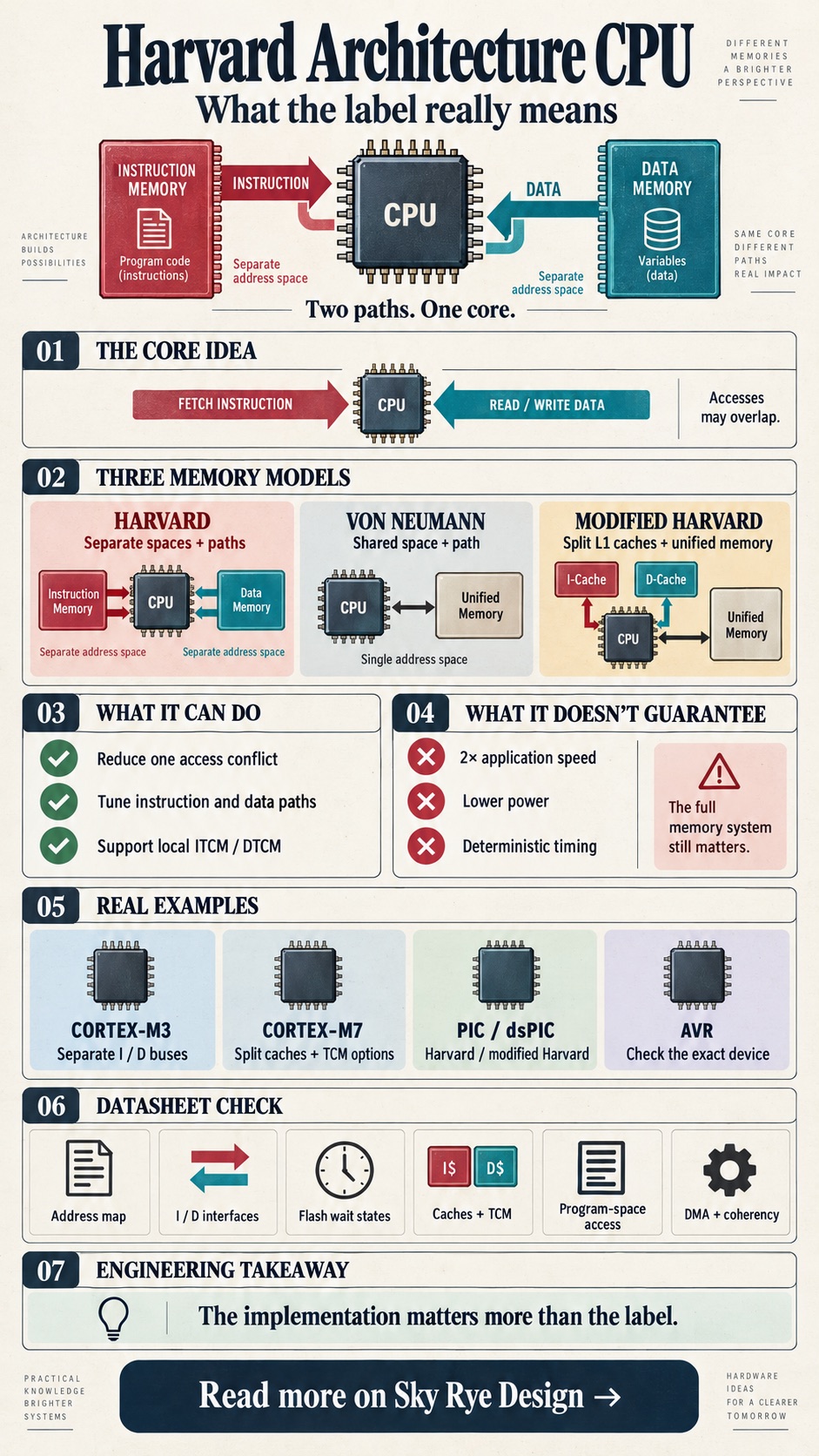
In a pure Harvard machine, program and data memories are physically and logically separate. Software may use different instructions or pointer types to reach them. A modified Harvard processor relaxes that separation. It might expose one unified address space to software but retain independent instruction and data caches, ports, or TCMs close to the core.
That hybrid is common because it combines a convenient programming model with parallel local access. It also creates a practical issue: writing bytes through the data path does not guarantee that the instruction cache immediately sees them. Arm’s guidance on caches and self-modifying code explains why software may need to clean data-cache entries and invalidate instruction-cache entries before executing updated code.
Real processor examples
Arm Cortex-M3 and Cortex-M7
Cortex-M3 is a clear example of a core with separate instruction and data interfaces. Cortex-M7 extends the idea with configurable instruction/data caches and TCM options. The exact memory behavior of a microcontroller built around either core still depends on the chip vendor’s flash accelerator, SRAM banks, bus matrix, and peripheral map.
Microchip PIC and dsPIC devices
Microchip describes dsPIC and PIC24 devices as modified Harvard machines with separate program and data memory spaces. Its documentation also describes Program Space Visibility, a window that lets data-space operations access part of program space. That is a good example of a modified design solving a practical problem rather than enforcing absolute separation. See Microchip’s dsPIC address-space documentation.
Not every microcontroller uses Harvard architecture
“Microcontroller” is a product category, not a memory architecture. Microchip’s simulator documentation distinguishes PIC Harvard devices, dsPIC/PIC24 modified Harvard devices, and 8-bit AVR devices modeled with Von Neumann architecture. That official processor-model comparison is a useful warning against generalizing from one family to every embedded chip.
How to identify the architecture in a data sheet
Marketing summaries may say “Harvard,” “modified Harvard,” or nothing at all. The block diagram and programmer’s model tell you more. Use this checklist before making a performance or software assumption:
- Inspect the address map. Are code and data in different spaces, or in one unified map?
- Trace the core interfaces. Look for separate I-Code, D-Code, instruction, data, cache, flash, SRAM, or TCM ports.
- Check access rules. Can ordinary loads read program memory? Can the processor execute from SRAM? Are special instructions required?
- Read the cache-maintenance section. Pay special attention to DMA, self-programming flash, bootloaders, and generated code.
- Review memory timing. Flash wait states, cache misses, shared buses, and arbitration can outweigh the simple architectural model.
- Confirm toolchain placement. Verify linker regions, section attributes, and library support for constants or program-space data.
This hardware layer also affects products people experience as design. A smart appliance interface, vehicle display, or connected device sits above processors, memory, and timing constraints. For the wider product context, read what digital design includes, then compare applications in self-driving vehicle systems and AI-enabled everyday devices.
Common misconceptions
“Harvard” describes a university-themed computer
The term is historical, not visual. A page about Harvard architecture should show memory paths, buses, caches, and processors—not campus buildings. The relevant entity is a computer architecture.
Separate paths mean twice the speed
They can permit two kinds of access at once, but one cycle is not the same as twice the total application performance. Execution units, branch behavior, cache misses, external memory, and dependencies may dominate.
Separate caches mean separate main memory
Not necessarily. Split L1 instruction and data caches can sit above a unified address space and shared lower-level memory. That is one of the most common modified Harvard arrangements.
The architecture guarantees deterministic timing
Separate local memories can make timing analysis easier, but determinism is a system property. Caches, buses, interrupts, DMA, peripherals, and software scheduling still matter.
Harvard architecture FAQ
What is Harvard architecture in computing?
Harvard architecture is a processor organization with separate instruction and data address spaces and access paths. That separation can let the processor fetch an instruction while it reads or writes data, although the real performance gain depends on the complete memory system and the workload.
How is Harvard architecture different from Von Neumann architecture?
A classic Harvard machine keeps instructions and data in separate memories with separate paths. A classic Von Neumann machine uses one shared memory space and path. Many modern processors combine the ideas by using separate instruction and data caches over unified main memory.
Does Harvard architecture always use two physical memories?
No. A pure Harvard design uses physically separate program and data memories. A modified Harvard design may present one programmer-visible address space while using separate instruction and data caches or tightly coupled memories inside the processor.
Are all microcontrollers Harvard architecture?
No. Microcontrollers use several organizations. Some PIC and dsPIC devices use Harvard or modified Harvard designs, while Microchip documents its 8-bit AVR simulator model as Von Neumann. Always check the specific device data sheet and programming manual.
Why do modified Harvard processors need cache maintenance?
Instruction and data caches can hold different copies of the same memory. Code that writes new instructions through the data side may need to clean the data cache and invalidate the instruction cache before execution so the processor fetches the updated bytes.
A practical conclusion
A Harvard architecture CPU separates instruction and data access so a processor can serve both streams without forcing every request through one interface. The idea is valuable, but the implementation matters more than the label. Identify whether the device is pure or modified Harvard, map the interfaces through the cache and memory hierarchy, and verify the software rules in the vendor documentation before drawing conclusions about speed, power, or real-time behavior.
- 94shares
- Facebook0
- Pinterest94
- Twitter0
- Reddit0